Before the pandemic, conflict in Ukraine, and trade tension with China, supply chain risk management was a topic that mostly interested eager business students and industry scholars. Back then, most businesses didn’t have to contend with much risk in supply chains, and rarely worried about delays or shortages of needed parts.
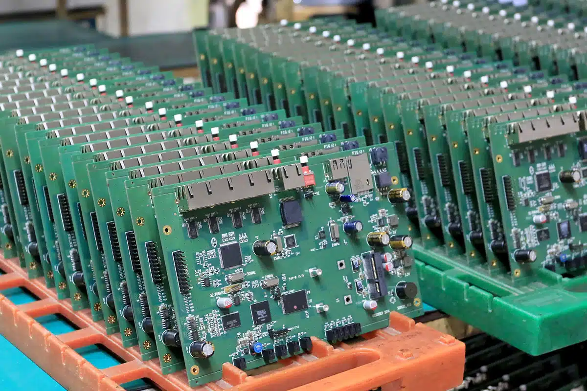
Then came the pandemic and its aftermath, and along with it, broken supply chains. And those supply chains that didn’t break still strained to deliver raw materials and other inputs. The most visible sector to be hit by these shortages was the automotive industry. S&P Global Mobility estimated that there were 9.5 million fewer light vehicles produced in 2021 because of the lack of semiconductors. But the electronics industry—though it didn’t make the same headlines—also suffered. And those shortages have had a lasting effect.
No Return to the Status Quo for Supply Chain Risk Management
Savvy manufacturers are recognizing that preparation is the key to flexibility, and are creating contingency plans and crisis-response infrastructures that enable them to better manage supply chain risks.
Compared to their predecessors, today’s electronic devices are chip hogs. So while semiconductor manufacturers continue to ramp up capacity, especially here in the U.S., some electronics companies still find themselves redesigning products to make use of more readily available components. It’s this type of scenario that makes supply chain risk management more than just an academic exercise.
It’s highly unlikely that supply chain risk management will ever return to the business-as-usual approach of the pre-pandemic years. Industry leaders surveyed for a recent McKinsey & Company report made it clear they have no intention of returning to the status quo ante. New trends and approaches are now emerging in response to lessons learned during the pandemic years.
Trend #1: The Shift from “Just-in-Time” to “Just-in-Case”
Electronics companies have long pursued efficiency and cost-reduction strategies, and were early adopters of “just-in-time” manufacturing when the concept arrived on America’s shores in the early ‘80s. For many years, companies competed to see how far they could push this lean manufacturing model in their quest to eliminate waste, and some began carrying very low parts inventories. By reducing the number of components sitting in their warehouses, these companies were able to minimize storage costs, maximize efficiency, and reap higher profits. It was a flawless system—provided there were no disruptions.

However, this lean-and-mean model was vulnerable to hiccups. That wasn’t a problem when supply disruptions were few and far between. But then the pandemic came, and the dominos began to fall. China adopted a zero-covid policy and closed ports when there was an outbreak, disrupting chip supplies the world over. Then came the Ukraine-Russia war, which disrupted global supplies of neon (used in chipmaking lasers) along with palladium, cobalt, and nickel.
As a result of these and other disruptions, electronics manufacturers found themselves scrambling for new suppliers, and sometimes, even redesigning their products to rely on more readily available components. These companies had bumped up against a non-negotiable reality: Lean manufacturing practices, while ideal during times of robust supply chains, sacrifice resilience for efficiency. And supply chains are no longer as reliable as they once were.
After being burned by the “just-in-time” approach in the last few years, many companies are now shifting to a new strategy: the “just-in-case” model. Keeping extra materials on hand costs more and can lead to excess stock or obsolescence. However, many companies today are accepting these risks to offset the chance they will experience severe shortages. Despite the elevated costs of this new approach, experts anticipate that companies will continue to follow this path for at least a few more years, unless and until global supply chains stabilize.
Now the pressing question for electronics companies is: How many component parts should they keep on hand? And how best to manage that inventory? This is one reason why it’s increasingly important to work with a manufacturing partner with expertise in supply chain management and inventory control.
Trend #2: Bringing Manufacturing Back to America
The just-in-time approach was not the only strategy that made companies vulnerable when supply chain disruptions hit. Many American companies sourced from the Far East—an approach that quickly became problematic during global disruptions. Sourcing so far from their primary markets left little leeway for error, and many companies faced huge shipment delays—first in Asia, then in Europe, and then in regions of South America. Country-specific tax and trade regulations added to shipping timeline woes, slowing delivery of much-needed parts. Budget concerns also plagued companies as international shippers dramatically increased prices. For example, during the pandemic, the cost of shipping a forty-foot container rose from about $1,300 to more than $11,000, before returning to its current average of about $4,000.

As these circumstances unfolded, American companies began seeking ways to reduce exposure to supply chain risk. Many businesses began exploring their options for doing business closer to home. According to the BCI Supply Chain Resilience Report 2020, 66.2% of organizations reported planning to source their goods and inputs more locally.
In addition to timing and budget concerns, companies have faced other challenges: rising labor costs worldwide, growing political instability in certain exporting countries, and trade wars that result in unpredictable tariff increases. These disruptive developments are leading many companies to rethink their global manufacturing strategies and seek reshoring partners.
Another reason many U.S. manufacturers are seeking to source and build closer to home is the threat of intellectual property (IP) theft. Chinese manufacturing partners are generally considered the riskiest in this regard. According to the U.S. Patent and Trademark Office (USPTO), “U.S. companies doing business in China face a range of challenges in protecting and enforcing their intellectual property (IP).” But while China may be the most well-known country in this regard, IP theft is a global phenomenon, making domestic production the safest option for IP protection.
Trend #3: Flexibility and Preparation Become Critical
The overwhelming majority of respondents in the above-referenced McKinsey report said that recent global crises have revealed weaknesses in their supply chains. One of those weaknesses was relying on a sole supplier, an approach that many manufacturers have begun to rethink. According to a survey conducted the Cybersecurity and Infrastructure Security Agency (CISA), 57.2% of respondents planned to diversify their supplier base post-pandemic.
Manufacturers have also recognized that they can reduce supply chain risk if their PCBA designs are more flexible; that is, if they can use the same components for multiple functions, or conversely, use different components to achieve the same result.
Savvy manufacturers are also recognizing that preparation is the key to flexibility, and so are creating contingency plans and crisis-response infrastructures that enable them to better manage supply chain disruptions. These forward-thinking businesses have planned for a wide variety of “what-if” scenarios, with the goal of compensating for material shortages and distribution bottlenecks without missing a beat.
Trend #4: Optimizing Inventory and Distribution Technology
Taking advantage of current technology is critical for optimizing the end-to-end management of any supply chain. Respondents in the McKinsey report saw an urgent need to gain better control of their supply-chain technology, a goal which will require a skilled workforce trained to use new digital tools. It’s not surprising that 90% of industry leaders surveyed said they planned to increase their organizations’ supply chain talent through in-house reskilling and external hires.
Another way companies are choosing to optimize their supply chain operations is by increasing supply chain visibility and control through the Industrial Internet of Things (IIoT) and other technologies. For example, automating the warehouse, back office, and transportation network allows a company to know precisely when its components and other inputs arrive and in what condition. And it lets these same companies monitor where their finished products are in transit, when the customer receives them, and in what condition. A relatively new IIoT technology, known as Multi-Dimensional Monitoring (MDM) can provide real-time tracking that generates notifications for all stakeholders along the supply chain.
Every new advance has its tradeoffs, however. While increased automation does enable electronics companies to better manage both material inputs and finished products, this same technology also brings an increased risk of malware, ransomware, phishing, hacking, and data breaches. Cyberthreats have grown steadily over the past few years, and these threats escalated as businesses connected their systems directly to their growing base of suppliers.
According to CyberGRX, a cybersecurity management company, 82% of organizations have experienced one or more data breaches caused by a third party—at an average cost of $7.5 million per incident. Any vendor that interacts with your systems is a risk. The answer, however, is not a return to clipboards and hand counting. Rather, companies should carefully vet their suppliers—not just to make sure those suppliers are trustworthy, but also to ensure that these vendors’ systems are as hack-proof as possible. It’s prudent to remember that vendor systems that connect to your company network are in a sense part of your network—and your cybersecurity is only as robust as the weakest link.
Trend #5: Looking Beyond Supply Chain Risk Management
Managing a company’s supply chain isn’t simply about risk mitigation. As more and more companies are discovering, it’s possible to use the supply chain to achieve secondary, yet highly valuable, goals. Companies seeking to up their ESG score, for example, can use their supply chain to promote both diversity and sustainability, simply by considering these factors in choosing their vendors. If your vendor has a high ESG score, it can help increase your own.
Quality, efficiency, reliability, and cost-effectiveness will always be a company’s primary considerations. Fortunately, however, these days there are many suppliers that can deliver on these requirements along with the diversity and sustainability you need to help you meet your own ESG goals. So be sure to ask about these issues when vetting your suppliers. With just a little extra effort, your company will be able to meet its ESG goals while effectively addressing supply chain risk management.