In 1954, the first robotics patent was filed by George Devol, affectionately known as the “grandfather of robotics.” In 1956, together with Joseph Engleberger, Devol founded the first robotics company, Unimation. Five years later, Unimation’s first robot—aptly named Unimate—was installed at a GM plant where it was programmed to retrieve and stack hot die-cast metal pieces, saving human workers from the risk of burns. Soon, Unimation expanded to include industrial robots that could print, weld, and assemble.
Devol’s patent for a programmable robotic arm became the foundation of our modern robotics industry. Today, according to the International Federation of Robotics, there are approximately 3.9 million industrial robots worldwide. Statista estimates that the global robotics industry will hit $43.32 billion in revenue in 2027, compared to just $18.47 billion in 2016.
The Benefits of Industrial Robots in Electronics Manufacturing
Current trends point to electronics manufacturing becoming the largest market for industrial and collaborative robots in the near future.
The demand for industrial robots is rising in many industries, including electronics manufacturing, which currently accounts for 22% of total robot shipments. This is second only to the automotive industry, which accounts for 33%, according to Supplyframe. But while the automotive industry has been the major consumer of industrial robots for a long time, Supplyframe reports that current trends point to electronics manufacturing becoming the largest market for industrial and collaborative robots in the near future. This development is not surprising, as industrial robots offer electronics manufacturers a host of advantages.
Ability to Tackle Complex or Delicate Tasks
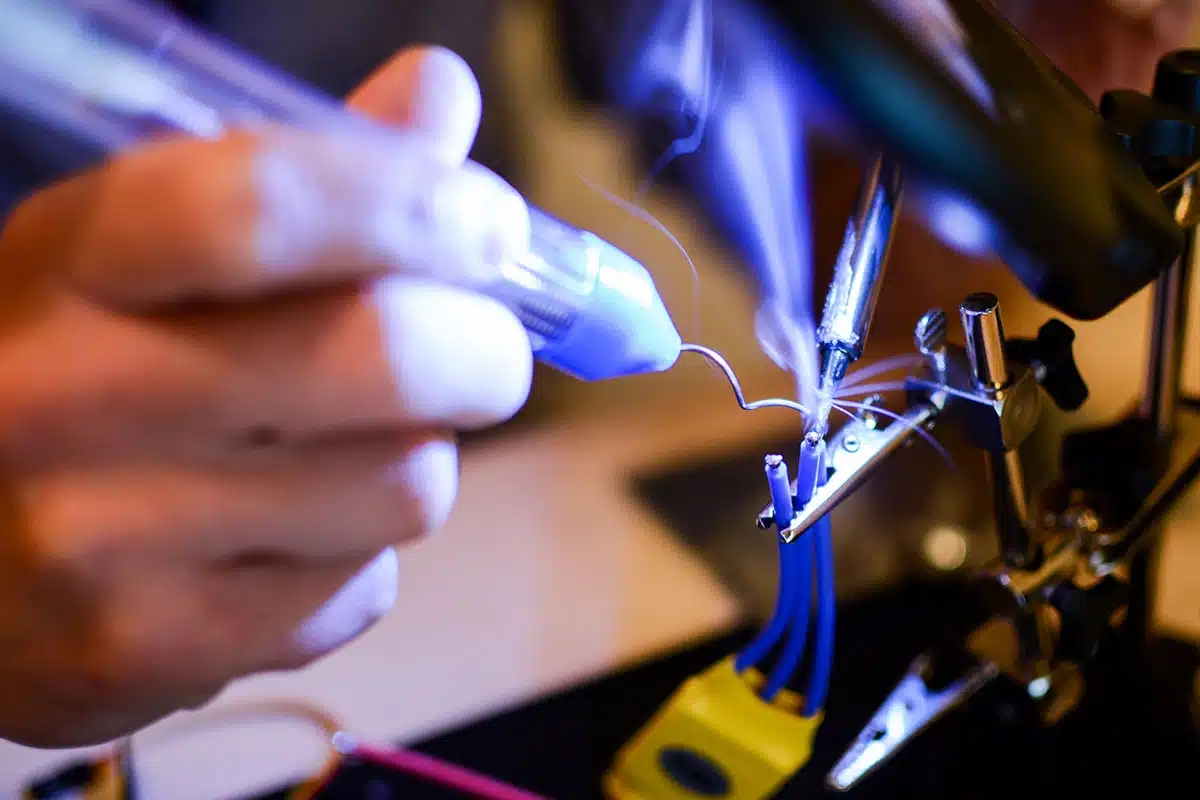
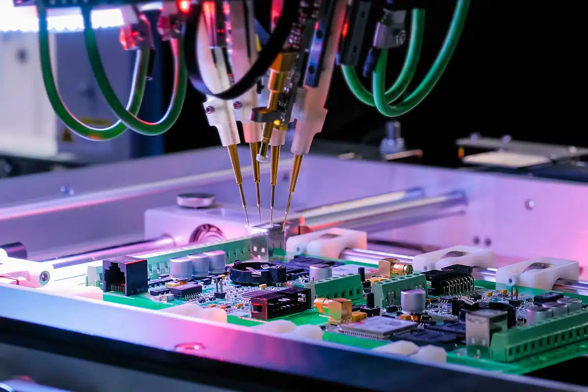
As components and circuits continue to shrink, and component density rises, human technicians are encountering physical limitations. Automated robots, on the other hand, support miniaturization. They can build connectors, subassemblies, display screens, and more—safely handling electronic components of any size. Robots equipped with force and tactile sensors, for example, can place even delicate components precisely and quickly, speeding up the coating and assembly of PCBAs and finished products.
Accuracy and Speed
For the moment, humans are still able to navigate the challenges of miniaturization, component fragility, and task-to-task variability. But they are often no match for robots when it comes to speed in assembly and testing. Humans are also more likely to introduce errors, waste, and inefficiencies. Industrial robots equipped with sophisticated imaging technology and AI software, on the other hand, can efficiently perform both inspection and pick-and-place operations with an extremely low error rate.
Consistency and Dependability
Unlike humans, industrial robots can repeat the same task over and over without getting tired, taking a break, or making a mistake. They can also work beyond an eight-hour shift with no overtime pay required. Industrial robots are also more consistent, able to perform the same function over and over without variation—producing thousands of PCBAs, for example, that are identical.
Flexibility
Modern robots aren’t just more precise than their predecessors—they’re also more adaptable. Today’s robotic arms are flexible and lightweight, and can easily adapt to multiple applications, saving manufacturers both time and space. When product designs change, smart robots don’t require replacing; reprogramming and swapping out a few parts, such as an arm attachment, is often all that’s required.
Workplace Safety
Workers can also benefit from automation, especially when it comes to workplace safety. Electronics manufacturing involves the use of numerous potentially hazardous heavy metals and other materials. Robots can help reduce workers’ exposure to these materials by taking over coating and other tasks that require the use of chemicals. And when it comes to assembling the finished product, robots can also eliminate the need for workers to repeat ergonomically problematic movements.
Cost
Many steps in electronics production—including component fabrication, PCBA assembly, adhesive application, inspections, packing, etc.—are repetitive tasks. This makes them ideal for automation. Using robots to perform these functions doesn’t just save on labor costs; it also reduces the errors that lead to costly manufacturing waste.
Three Trends in Industrial Robotics
Human inefficiencies have a cost. So, an automated solution that can simultaneously improve product quality while lowering overall unit cost is a boon to manufacturers. In many cases, industrial robots provide that solution.
Electronics manufacturers are recognizing these benefits. In a survey of industry leaders by trend-spotting company Exploding Topics, 97% listed improved product quality as a clear benefit. Additionally, 95% mentioned faster production speeds, and 92% cited greater production capacity.
Around the world, companies are embracing automation. In fact, McKinsey & Company reports that many companies will dedicate 25% of their capital spending over the next few years to automated systems, with the goal of improving output quality, efficiency, and uptime. This global trend in robotics adoption is due to the expanding capabilities of today’s industrial robots, which are being fueled by three major technological advances.
Machine Learning and Artificial Intelligence (AI)
Sometimes the terms “AI” and “robotics” are used interchangeably, but they are two different technologies. Robotics is the science of designing and building physical robots to perform automation. AI, on the other hand, focuses on how to create machines and technology that mimic human intellectual capabilities.
The two worlds, however, have a lot of overlap. Some robots now allow users to program them using natural language instead of code. This advance is a big one, as it removes the need for workers with specialized programming skills. And in some cases, the need for humans is even further reduced. It’s possible to build a factory that’s so automated that a human need enter the premises only once every few weeks. Known as “lights-out manufacturing,” this approach to production is nearly fully automatic. For example, FANUC, a Japanese robotics company, operates a factory where robots can run unsupervised for up to 30 days at a time.
Cobots
Have you ever felt like you could use an extra pair of hands to perform a task? A cobot, also known as a collaborative robot, provides that option. Cobots are designed to work alongside humans and are one of the fastest-growing segments of the industry. They are especially useful for small companies that cannot afford or do not want to deploy a fully integrated robotic system.
Mobile Manipulators
Mobile manipulators—also known as “MoMas”—combine the mobility of robotic platforms with the dexterity of manipulator arms. The mobile platform extends the workspace of the arm, while the arm itself offers the necessary functional operations. Using cameras and sensors, these robots can perform maintenance tasks and inspections on equipment.
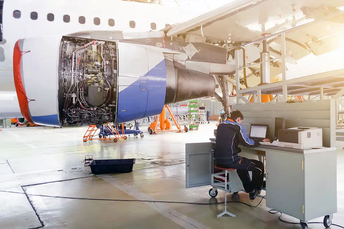
With their ability to support human workers, MoMas are being used across a large spectrum of industries. For example, in the aerospace and defense sector, they can perform such tasks as aircraft assembly, inspection, and maintenance. Some of their benefits in this sector include the ability to handle delicate components, maneuver in confined spaces, and perform precise operations.
MoMas are also bringing further automation to the car industry. As automotive electronics become increasingly sophisticated, car manufacturers are looking for ways to be more efficient. Mobile manipulators are ideally suited for such tasks as assembly, transport of components, and quality checks. Using this advanced technology, car manufacturers can improve product quality as well as production speed.
Given their myriad applications, and the ongoing labor shortage, it’s no surprise that MoMas are gaining in popularity across these and other industries.
When Not to Use Industrial Robots
While industrial robots bring many benefits, there are situations in which companies would be wise to think twice before investing in this capital-intensive technology. Here are a few caveats to keep in mind.
Cost
While industrial robots can certainly save money in the right situations, just the opposite is true in some cases. Companies, therefore, need to perform their due diligence by conducting a cost-benefit analysis. Humans can be less expensive—and reliable enough to produce a high-quality product. The fact is, installing industrial robots entails a high capital outlay. And in some cases, a cost-benefit analysis will reveal that the return on investment does not justify the expense incurred. In these cases, it’s good to keep in mind that there are other ways to save time and money in electronics manufacturing.
Complexity
A lack of experience with automation can pose a significant hurdle for many companies, especially those that are small or mid-sized. Even if you have the capital to install the system, do you have personnel with the expertise to operate and maintain such a system? While generally enthusiastic, McKinsey found several concerns about the adoption of industrial robots, including how to fit the machines into existing spaces, and the ability of the robots to interface with existing production processes.
Cybersecurity Risks
Stories of cyberattacks, across multiple industries, are plentiful in the news today, leading to widespread concern about automation and the misuse of AI. According to the AIAAIC, the number of AI incidents and controversies recorded in its database is now 26 times greater than it was in 2012. And companies have noticed—McKinsey found that cybersecurity concerns sometimes deter manufacturers from the use of robotics.
Should You Invest in Industrial Robots?
So how does a manufacturer decide whether or not to pursue industrial robots as part of their manufacturing plan? As with so many things, it depends on your company’s unique situation. For some manufacturers, a more hands-on approach will be optimal. Depending on the manufacturing steps, humans may be able to move more efficiently from one task to another than robots that require refitting or reprogramming. If you manufacture a broad range of products, would automating your factory floor require a plethora of specialized robots?
It can take a lot to figure out the right balance between robots and humans. Fortunately, you may not need to decide. One way to keep it simple—and avoid a high capital outlay—is to hire a contract manufacturer who has already figured out how to get the job done in the most efficient and cost-effective way.