Thinner boards. More powerful components. Denser layouts. Today’s assembled PCBs are increasingly complex and require thorough and accurate testing to ensure they perform as expected. That’s why, when it comes to getting your product to market, design for test (DFT) is crucial to the manufacturing process. Incorporating DFT principles into the production of your device increases the certainty of your product’s reliability, efficiency, and ultimately, commercial success.
What is Design for Test and Why is It Important?
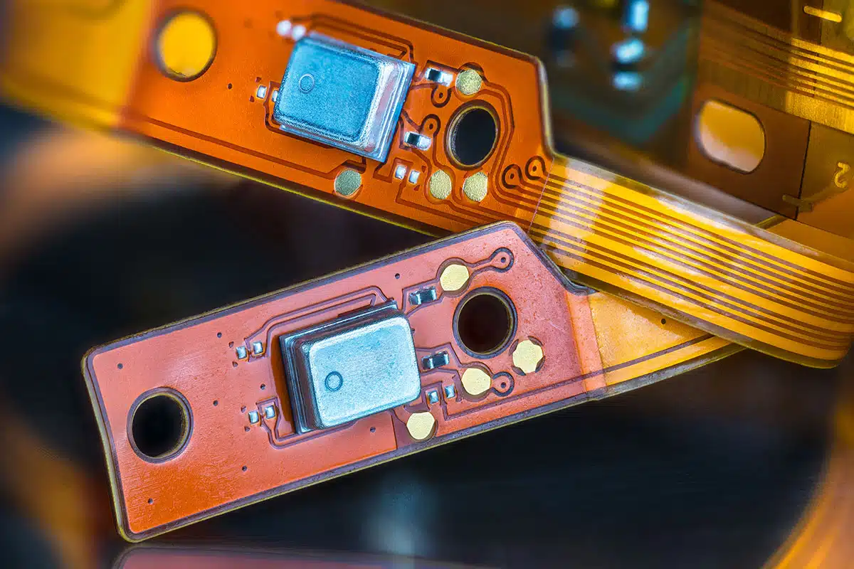
Testing is an integral part of the electronic manufacturing process. Without it, failure points, power inefficiencies, and reduced functionality in a product can go undetected. Testing can produce valuable system information, providing engineers with opportunities to increase the product’s functionality and performance for the consumer.
Taking the trouble to incorporate DFT principles into your design is an investment that will yield benefits throughout the life of your product.
Designing your electronics device using DFT protocols makes it possible to efficiently and cost-effectively test the product—even after it has been assembled. DFT-savvy engineers can create designs for PCB assemblies that ensure easy testing, with test points that are properly spaced and with enough surface area to give accurate and reliable readings quickly and easily.
Taking the trouble to incorporate DFT principles into your design is an investment that will yield benefits throughout the life of your product—beginning with the detection of design flaws and ending with a satisfied customer.
DFT for Defect Detection
Testing ensures that your product is free of faults and malfunctions and delivers a customer experience that leads to repeat sales.
To ensure a high-quality experience for the end user, it’s important to test your device at multiple stages. Start by virtually testing your design. You’ll want to test each prototype as well, since that’s the best time to work out any real-world issues that weren’t caught during the initial design. Periodic testing should also be conducted during the manufacturing process, to ensure that the product coming off the line is performing to expectations at each stage.
It can even make sense to test after the sale. If a product is returned from a dissatisfied customer, testing will allow you to find any residual flaws that are affecting your product’s durability or performance. If such a flaw is found, it may make sense to tweak the manufacturing process. Testing will give you the information to determine if the benefits of a manufacturing change will outweigh the costs.

Provide Data
Recently the engineers at Space X cheered when the Starship rocket spectacularly exploded shortly after takeoff. It seems no one was upset at the sight of billions of dollars’ worth of material and effort going up in smoke. Why? The data. As one of the engineers said: “Success comes from what we learn, and today’s test will help us improve Starship’s reliability.”
Information and data are essential. The benefit of DFT is not just the ability to detect and correct faults, but also to gather critical data that can inform the design of your product’s next iteration. It can allow you to spot weaknesses that can be designed out, or discover ways to increase the power of certain features.
Fortunately for electronics companies, DFT in manufacturing does not require any explosions. But as with space vehicles, it’s important to carefully analyze product failures. Determining what went wrong can yield precious data and allow you to better design your product’s next upgrade. Data gained from DFT can be used to develop new manufacturing procedures, refine features, and produce a more robust product.
Lowering Costs
When manufacturing any electronic product, costs need to be controlled, while quality, durability, and functionality must be maintained. Although testing procedures may initially impact production costs (depending on the complexity of an assembled PCB), testing provides significant savings in the long term. Including test points makes it possible to accurately identify the location and nature of a fault within a system and speeds up troubleshooting. And an experienced engineer can find the optimal placement and use of these test points.
For example, although test points can be located on either the top or bottom of the PCB (so long as they don’t interfere with other electromechanical components), having them on both sides requires the manufacturer to create a clamshell fixture. This approach is expensive, and less accurate than the ideal.
Usually, the better testing strategy is to put test points on one side only. This not only avoids the costs of the clamshell, but also increases accuracy, which in turn enables better batch quality prediction and a fast production time.
Incorporating DFT principles early in the design process will allow you to reap these and other benefits right from the start. Planning for testing, for example, allows you to avoid the expense of adding additional test points later in the production process once it’s become clear that they’re needed.
Compliance and Customer Satisfaction
Most consumers are unaware of the complexity of the assembled PCBs that power their products. But that doesn’t mean their expectations of quality and functionality are low. And of course, manufacturers and OEMs want safety and the very best quality for their customers.
Design for testability is not just about improved functionality and streamlined production. Safety, quality, and customer satisfaction are also key areas that can be improved with DFT. Standards and regulations required by governing agencies are built into the tests that each product must go through.
Even the simplest design has to comply with standards from numerous bodies, both state and federal. And if a device fails to meet regulatory standards, it will be much easier to discover the cause if the product was designed with testing in mind. In that case, it’s a straightforward process to determine which component failed, or which usage scenario created excess stress on the product—or worse, compromised safety or quality. A problem that is identified quickly can be rectified quickly.
Design for Test and for the Future
Electronic devices continue to evolve, as do the PCBs that form their backbone. Flexible PCBs, with their high heat resistance, are becoming more popular for wearable electronics and medical devices. Another trend in PCB construction is the use of biodegradable materials, spurred by consumer demand for greater sustainability. And in a related development, 3D printing—which produces less waste—is also making inroads into PCB production.
And as PCBs change, so will the ways to incorporate test points and other features that allow for the quick detection of flaws or failures. But what’s unlikely to change is the need to test both prototypes and finished products to ensure the best possible consumer experience.