Our Stories

“Our state is on track to lose 10% of its water supply by 2040.” So said California Governor Gavin Newsom in a speech announcing incentives to encourage the replacement of water-thirsty lawns with drought-tolerant landscaping. And California is not alone. One state over, the Nevada Legislature recently enacted a law prohibiting the use of irrigation for non-functional (i.e., purely ornamental) grass at commercial properties.

States are getting serious about water-wise landscaping and are making efforts to ensure outdoor spaces are more sustainable. This is apparent not only from the laws they’re passing, but also the cash rebates that many municipalities are offering to encourage owners and managers to transition their grounds to drought-tolerant landscaping. 

These rebates are just one of the many benefits of switching to eco-friendly grounds. Water conservation and reduced maintenance costs are two other plusses. To reap these benefits and make the most of sustainable grounds and landscapes, building owners and managers should keep the following methods and tools—and rebates—in mind.

Drought Tolerant Landscaping: It’s Not Turf

According to the Nevada Water Authority, approximately 825,000 gallons of water per year can be saved for every 15,000 square feet of land converted to water-smart landscaping.

Grass and lawns are the most water thirsty of landscaped areas. In fact, according to the Nevada Water Authority, approximately 825,000 gallons of water per year can be saved for every 15,000 square feet of land converted to water-smart landscaping. That’s a lot of water—and money—saved.

One way to create water-smart landscapes is to replace turf with xeriscape, terrain that requires little or no irrigation and is typically comprised of native and adaptive plants. These plants and shrubs naturally thrive in dry conditions. They’re also more resilient and can be as aesthetically pleasing as more water-thirsty options. Planting native or adapted plant species that are well-suited to the local climate also reduces the need for mowing, chemical applications, and other types of maintenance.

According to the Pacific Institute, commercial property managers can reduce landscape water use by 70% to 80% just by replacing turf with efficiently irrigated, climate-appropriate plants. Here are a few of the rebates available for turf replacement:

  • Southern Nevada Water Authority has a turf rebate program that offers rebates for businesses, HOAs, and multifamily properties. The rebate is $3 per square foot of grass that’s removed and replaced with desert landscaping and is available for up to 10,000 square feet of landscape per fiscal year.
  • Southern California’s West Basin Municipal Water District is offering rebates starting at $4 per square foot to remove non-essential grass on public properties in their service area. This offer includes free professional advice to help design new, water-wise landscapes. Any federal, state, or city property in the district’s area may qualify for rebates on parcels that range from 250 square feet to 200,00 square feet, with a maximum rebate value of $800,000.
  • The City of Sacramento offers Turf Conversion Rebates where you can convert to drought-tolerant landscaping and receive up to $1.50 per square foot of replaced turf (up to $50,000).

Smart Irrigation, Smart Savings

The first lawn sprinkler was patented in 1871, and it proved revolutionary in cementing the popularity of grass lawns—despite its inefficient design. Since then, the humble sprinkler has undergone several improvements, including the oscillating sprinkler in 1948 and the introduction of time-based controls in the 1960s. Yet studies show that despite these advancements, as much as 50% of the water used by modern sprinklers is wasted through overwatering. But new advances in sprinkler technology are changing that. 

Smart irrigation controllers are among these game-changing technologies. Far more effective than time-based control, smart irrigation controllers optimize water use by employing advanced technology and data analysis. They consider factors such as weather conditions, soil moisture levels, and plant water requirements to ensure precise and efficient irrigation. Most smart irrigation controllers are either weather based or soil moisture based. Both types can tailor watering schedules and run times for a sprinkler or drip system.

Weather-based controllers use various signal technologies to gather temperature, humidity, and even solar radiation readings (typically from a local weather station). The controllers use this data to automatically adjust irrigation schedules, ensuring the landscape receives the optimal amount of water for the current climate conditions.

A local controller for a smart irrigation system
Smart irrigation controllers use data about weather and soil conditions to adjust watering schedules.

Soil moisture-based controllers, on the other hand, take a more direct approach. These controllers utilize soil moisture sensors, placed underground, to gather data from the root zone of plants. The sensors estimate the soil volumetric water content—the portion of the total volume of soil occupied by water—and adjust watering accordingly.

The water-saving potential of these smart irrigation controllers and sensors is substantial, as was powerfully demonstrated by an EPA study of an office complex in Plano, Texas. The owners of the complex installed a weather-based irrigation controller, along with rain and freeze sensors. In addition, they committed to regular maintenance and repair work. The EPA study found that after these changes, the complex reduced its water use by 12.5 million gallons of water in the first year alone, for a savings of $47,000. The upgrades paid for themselves in only 1.5 years.  

Currently there are multiple local and regional agencies offering rebates on both weather-based and soil moisture-based irrigation controllers, including these water districts:

  • In Utah, the Washington County Water Conservancy District has a $75 rebate for irrigation smart controllers.
  • The Santa Clara Water District offers up to $50 for rain sensors and between $300 and $2000 (depending on the number of stations) for weather-based irrigation controllers.
  • The Metropolitan Water District of Southern California offers rebates of $35 per station for irrigation soil sensors and weather sensors as part of its Water$mart program. This program covers parts of Los Angeles, Orange, San Diego, Riverside, Ventura, and San Bernardino counties.
  • In Texas, the Water Wise Austin program offers rebates of $300 each for flow sensors, electronic devices that measure and regulate the flow rate of water within pipes, a critical technology for conservation. The program also covers 50% of the equipment cost, per station, for central computer irrigation controller systems, up to $10,000.

Irrigation Drip Systems

While most sprinkler systems could benefit from an upgrade, one approach to watering has long been known to be highly efficient: drip irrigation. This type of irrigation, which has existed for decades in one form or another, exceeds 90% efficiency, making it an effective, well-established technology for reducing overall water use. Drip systems are especially effective for sloped areas, due to the slow rate of water application. In these instances, the water soaks in instead of running off, avoiding soil erosion and water waste.

Although, just like sprinklers, drip systems do need monitoring and maintenance (to ensure they don’t become clogged or spring leaks), they offer other advantages in addition to cost savings:

Drip irrigation systems reduce water loss due to wind, evaporation, or watering of non-plant areas.
  • Soil Moisture Retention: By providing water directly to the root zone, drip irrigation helps maintain consistent soil moisture levels, preventing excessive drying or waterlogging. Maintaining optimal soil moisture levels in this way contributes to the resilience of plants during drought conditions.
  • Weed Control: Another advantage of drip irrigation systems is that they enable highly targeted watering, which works to starve weeds of water and cuts back on their growth. This in turn reduces maintenance costs.
  • Preventing Foliar Diseases: Overhead irrigation methods can lead to moisture accumulation on plant foliage, creating a favorable environment for the development of fungal diseases. Drip systems prevent excessive moisture on leaves, reducing the risk of foliar diseases and promoting healthier plants.
  • Landscape Design Flexibility: Inline drip systems offer flexibility in landscape design and installation. The tubing can be easily laid out in various patterns, allowing precise customization for different plant types, spacing, and landscape configurations.

We found these municipalities offering rebates on drip systems that may suit your landscape:

  • Municipal Water District of Orange County (MWDOC) offers rebates for businesses to convert areas irrigated by spray heads to drip irrigation. Rebates are at $0.50 per square foot of converted area, with a maximum of 50,000 square feet for each qualified customer.
  • Cal Water Conservation Rebate program offers $0.50 per square foot of landscape for spray-to-drip irrigation conversion for multi-family residential and non-residential customers; the maximum rebate is $5,000 for converting 10,000 square feet of landscape.
  • SVC Water is offering commercial customers in the Santa Clarita area $0.75 per square foot for spray-to-drip conversions.

Reap the Benefits of Drought-Tolerant Landscaping

No matter the size of a company’s landscaped terrain, customers and tenants appreciate organizations that embrace sustainability. This means that in following water-wise landscaping practices, companies not only lower their water and maintenance costs, they also please their customer base and burnish their corporate image.

Your Best Landscape

Whether you want to maintain the grounds you already have, or transition to more sustainable terrain, our grounds and landscaping team has the expertise to make your landscapes bloom. Contact us today to learn more about our award-winning services.

From optimizing energy consumption to streamlining maintenance processes, facility engineers play a pivotal role in generating cost savings for businesses and building owners. And although operations vary across industries, there are several fundamental areas where facilities engineering is crucial for optimizing operational efficiency, leading to significant cost reductions.

Here we take a closer look at the benefits that facilities engineering can provide owners and occupants for buildings and their operations across industries.

Maintenance Planning: Extending Asset Lifespan, Minimizing Downtime

In 2018, the U.S. Energy Information Administration (EIA) conducted a survey of the country’s building stock. The survey, known as the CBECS (Commercial Buildings Energy Consumption Survey), found that the median construction date of commercial buildings in the U.S. is 1981, with 50% of building stock having been built between 1960 and 1999.

A 400-ton water-cooled chiller operating year-round at a 30% load requires almost 1.9 million gallons of makeup water just to replace evaporation losses.

While it’s no secret that regular maintenance services can extend equipment and building lifespans, reduce downtime, and avoid costly emergency repairs, with such a large stock of older buildings, preventative maintenance needs to be more strategic than ever.

Maintenance from facilities engineering teams that is planned instead of reactive, predictive instead of catch-up, is the optimum approach to smooth building operations, especially for older buildings. In addition to keeping these buildings in check and preventing repairs from becoming replacements, facilities management and engineering that is preventative will also have less negative impact on staff productivity—cutting costs in two ways.

Repairs become replacements when maintenance is deferred. Unfortunately, just because repair is delayed doesn’t mean daily use by building occupants will stop. Take a malfunctioning water heater, for example. Fixing it as soon as it starts to fail keeps a minor repair from becoming and more time-consuming and costly replacement.

Maintenance planning includes regular and timely inspections of all equipment. This will reveal the minor defects that can turn into major problems if not addressed. Regular inspections can uncover things like blocked air returns, missing pipe insulation, and daylight sensors that have been inadvertently covered. 

Energy Efficiency: Facilities Engineering for Optimized Operations

From hospitality to healthcare, whether the facility is large or small, implementing energy-efficient measures can significantly reduce utility expenses and increase sustainability.

Across nearly all industries, heating and cooling systems account for as much as 30% of a building’s energy consumption. Engineers can ensure this energy use is continually optimized. Cleaning and maintaining filters, detecting and sealing air leaks (which cause the HVAC system to work harder), and ensuring thermostat settings are adjusted according to weather and building occupancy—all these efforts contribute to improving the building’s efficiency.

Lighting is another area where energy can be saved. Switching to LED products throughout a building can reduce energy consumption by as much as 60% compared to typical lighting. With more sustainable lighting, maintenance requirements drop significantly. LEDs are rated to last 50,000 to 100,000 hours, which—with typical office usage—means it will take 12 to 20 years before a bulb needs to be changed!

With skilled engineers in place, areas of energy inefficiency can be identified using an energy management system (EMS) that monitors and manages energy consumption in real time. If you already have a building automation system (BAS) in place to control electrical and mechanical equipment, you can take efficiency to a higher level by layering in an EMS to provide comprehensive data analysis and reporting. With this additional data, facility engineers can then adjust the BAS to optimize HVAC, lighting, power, and other systems, reducing energy waste and maximizing operational efficiency.

A uniformed technician checks panel readings for a large automated system.
Facility engineers can optimize building operations by analyzing data from BAS and EMS systems.

Commissioning

Even with expert technology-aided energy management, as buildings get older operations inevitably experience a “drift” from the optimum efficiency level of a new building or a building commissioned after a change of operations. This drift lowers efficiency and increases costs. To combat this, facilities engineering can conduct further commissioning audits (re- or retro-commissioning).

Through commissioning, operational inefficiencies are identified and necessary adjustments, fine-tuning, or equipment replacements are performed to reset the building operations to optimal performance. Commissioning outcomes not only save costs on energy but also contribute to occupant comfort and overall building performance.

Ideally, commissioning reviews should be conducted every five years. These reviews are essential for meeting the challenges that high-tech facilities such as data centers, healthcare facilities, and labs encounter; and they can be cost-effective even for small businesses.

An ongoing study (last updated in 2022) of Existing Building Commissioning (EBCx) by the Lawrence Berkeley National Laboratory found that increases in energy efficiency from commissioning saved facilities as much as 19% in energy costs. The research, which looked at 1482 buildings across the United States, showed a median simple payback time of 2.2 years. And based on the results of an earlier version of the study (2009), the energy savings continue for another three to five years.

Although commissioning can sometimes include a recommendation for retrofits, the study showed that over 80% of the energy savings achieved in the surveyed buildings were obtained by scheduling, operation and control changes, and modifying setpoints and advanced resets. But whether operational changes or retrofits, these are all measures that can be conducted by facility engineers and technicians.

Water Conservation

Water conservation saves money and resources—and it’s another area where facilities engineering can make a big difference. Facilities engineers play a key role in designing and implementing water-efficient technologies and practices, which reduce water consumption and its associated costs.

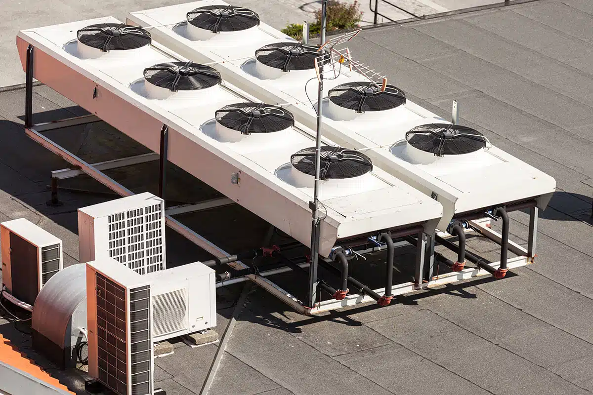
One of the largest consumers of water and energy in a typical commercial building is the HVAC system. Heating and cooling accounts for as much as 48% of a building’s total water use. Facilities engineering teams can take several steps to reduce this water usage and save owners money.

For closed looped systems and cooling towers, engineers can install water meters that help troubleshoot operational problems, track water usage, and enable the benchmarking of water efficiency improvement projects. Additionally, regular inspections by engineers are essential to identify and fix any leaks in closed systems, thus ensuring efficient water use and preventing waste.

An HVAC cooling tower system mounted on a roof
In a typical building, cooling and heating systems account for as much as 48% of the water use.

The water conservation techniques that are applied to HVAC cooling tower systems, which use water to evaporate and cool air, differ from the approach taken with closed looped systems. In water-cooled chillers, where the water that remains after evaporation is periodically drained and replaced, a lot of makeup water is needed. For example, a 400-ton water-cooled chiller operating year-round at a 30% load requires almost 1.9 million gallons of makeup water just to replace evaporation losses.

By exploring alternative water sources for use as makeup water for cooling towers, facilities engineers can conserve this essential resource. For example, condensate from fan coil units and air handlers can be used as tower makeup water. Gray water (reclaimed water that can be used for non-potable purposes) is another viable source. Even rainwater can be harvested from rain barrels or cisterns to serve as makeup water. By “reusing” water in this way, facilities can reduce the need for fresh water.

Scale buildup in areas with hard water is another cause of inefficient water use—and can even damage cooling towers. To minimize this scale buildup, facilities engineers can blend soft water with the area’s natural hard water. This improves efficiency and reduces water consumption.

Water conservation opportunities can be found in other parts of a building as well. In restrooms and kitchen facilities, for example, retrofitting the aerators on taps and replacing high flow toilets with low-flow versions can significantly reduce water consumption.

Wide-Reaching and Efficient

From the rooftop to the curb, across different sectors and industries, facilities engineering is vital to the smooth running of any building. By leveraging their expertise, facilities engineers can offer opportunities to drive cost savings, enhance operational efficiency, and ensure a sustainable future for commercial buildings.

A Partner You Can Rely On

Want to optimize the water and energy efficiency of your buildings? Our integrated facilities management team has been helping organizations do more with less for more than three decades. Contact us today to learn more.

Since the facility’s opening in 2013, the California Department of Corrections and Rehabilitation (CDCR) has struggled to find and retain a reliable, knowledgeable environmental services workforce for correctional and medical facilities. The unique nature of the organization and its facilities—its mission, its need for confidentiality, its sophisticated training requirements, its stringent cleaning requirements, its security clearance mandates, and the people skills required for patient interaction—presented significant challenges to delivering business excellence with a positive social impact.

A Reliable, Effective Workforce

“Before PRIDE Industries, CDCR used an inmate porter system, civil service personnel, and another contractor, but there were a lot of hiring and retention issues with all three,” said a Correctional Business Manager the department. “Then we found PRIDE Industries. Not only did their experience and expertise stand out, but so did their mission to create employment for people with disabilities.”

Beginning with environmental services at facilities in Stockton and Vacaville, in 2019 PRIDE Industries contract with CDCR expanded to the California Medical Facility (CMF), the healthcare service provider at both sites. CMF had experienced emergency environmental services shortfalls due to staffing shortages and put licensure, inmate and employing safety, and patient care at risk.

The PRIDE Industries team’s efforts and infrastructure also resulted in CMF reaching a Healthcare Assessment Maintenance score of 97.1% as of June 2022. These results point to measurable outcomes which preserve the facility’s licensure and its environment of care for patient housing and treatment, ultimately reducing the spread of disease and infection.

The 70 people with disabilities employed by PRIDE Industries at CDCR look forward to working every day. Unlike so many people with disabilities, workers at CHCR are able to experience the dignity of a paycheck and the satisfaction that comes with meaningful work. They’re inspired, and that inspiration has led to low turnover, low absenteeism, and diligent work practices—in other words, business excellence. Many of these employees have advanced in their careers from entry level roles to manager and director responsibilities.

Below, one of these dedicated employees describes her experience with PRIDE Industries at CMF means to them in her own words.

Patricia’s Story

Patricia Prescott has worked as an EVS technician at CMF since December 13, 2020.

I am an EVS tech. I go into the units that PRIDE Industries my company, cleans. We clean cells, offices, nurse stations, exam rooms and medication rooms, bathrooms. We also clean up floodings, and blood, pepper spray, poop, and on occasion vomit.

I like helping others out. I also enjoy cleaning. It relaxes me and helps me think. It’s also amazing exercise and you learn new things every day.

PRIDE Industries has helped me through some hard times. They’re an amazing company to work for. I am very thankful that they’re patient and understanding with my situation.

Some employers would never think about hiring people with disabilities because in their minds they aren’t capable of doing the job. The word “disability” is off-putting to employers. They have negative thoughts about people with disabilities.

They should take a chance on us and let us prove and show you that we are capable of doing the job. Believe in us, because what if that was you? Wouldn’t you want an employer to take a chance on you?

I am very thankful and appreciate PRIDE Industries. My husband is very sick and he’s in and out of the hospital. PRIDE Industries has been very supportive of me and has helped me out. I continue to have a job and I am able to provide for my family because PRIDE Industries is an amazing company. They understand what I am going through and have programs to help me. They offer me help when I need it. Most important, they hire people with disabilities. This company gives us chances to work, gives us opportunities to put ourselves out there trying new things that we think we were never able to do before.

I never once thought I’d step foot into a prison or let alone be working in one. I love my job and am very happy and thankful for it. I plan on staying and helping PRIDE Industries out just like they have helped me.

Business Excellence with a Positive Social Impacte

In just a few years, PRIDE Industries has helped CDCR and CMF move from having a hard time hiring and retaining employees with service shortfalls that put health, safety, and licensure at risk, to a thriving workforce and a stellar Healthcare Assessment Maintenance record. All the while, employees have experienced life-changing employment experiences.

Looking to make a social impact?

PRIDE Industries builds inclusive, diverse work environments where people with disabilities can thrive. Is your company seeking well-trained, reliable employees? Join our Employment Partner Network today to experience business excellence with a positive social impact.

From concept to consumer, there’s a lot involved in bringing an electronic product to market. At every stage—design, development, prototyping, production, and manufacture—careful planning is the key to success. This is why it’s essential to carefully plan out your fixture design for manufacturing and testing. Well-designed fixtures ensure reliable and streamlined production processes and ultimate customer satisfaction. And this is especially true when it comes to test fixtures.

Why Focus on Fixture Design for Electronic Manufacturing?

Fixtures enable consistent and repeatable positioning of components, allowing programmed tasks to be performed with precision and accuracy, and mitigating the possibility of bottlenecks in production. When your device is ready to be produced at volume, having the fixture designs already mapped out will mean higher efficiency and throughput.

From large medical or aerospace products, to small consumer electronics, every industry relies on testing to ensure quality and reliability.

For best results, fixture design for electronic manufacturing and testing requires the engineering and design skills of a professional engineering team that’s well-versed in both DFM (Design for Manufacturability) and DFT (Design for Testability) principles. These professionals will ensure that fixtures are designed and positioned for easy testing and optimal production efficiency.

Test Fixtures: Know the Objectives, Plan the Parameters

Achieving optimum results from any test fixture will require working with a qualified electronic manufacturing services (EMS) provider to plan the test fixture’s design with the specifications of the DUT (device under test) in mind—in addition to volume, turnaround, and budget considerations. While customization and planning may add time and some initial cost to the manufacturing process, this is offset by net time saving and cost reduction per item.

Test objectives, determined by industry standards, and the product’s final use and destination will define which test parameters should be incorporated into test fixtures and testing procedures. The test fixture customization and design are planned using CAD systems and software that set test points, calibration, and the collection of data specific to your product. Whatever level of testing you would like to perform, it’s important to consult with your EMS provider regarding the basic inspection requirements your device must satisfy.

Since determination of the fixture design will depend on the functionality and complexity of your device, there are cases where a simple test fixture with few test points and minimum customization—or even an “out of the box” fixture—will be sufficient. In other cases, a more complex test fixture—one that has to be precisely positioned and aligned—may be required.

The selection and deployment of test fixtures will also depend on factors such as production volume, size of the product, and desired quality standards, as well as the overall flow of the assembly process. Costs will also vary depending on the complexity of each fixture and the number of test points that are required. In general, simple test fixtures are less expensive than complex test fixtures.

A pair of engineers inspecting a prototype, with a large schematic on a display screen behind them
Testing can provide data specific to your device that can aid in its refinement.

Test fixtures will not eliminate test failures, as any manufacturing process has an inherent failure rate. However, tests designed with the help of skilled SMT engineers will catch faults early and minimize failure rates.

What Are the Benefits?

Although test fixtures for different devices and products will vary in the type and number of tests required, the overarching benefits of fixture design for electronic manufacturing are consistent:

Time and Cost Savings: Test fixtures streamline the testing process by automating test procedures and identifying defects early in the manufacturing process. With this fast and efficient testing, productivity is increased, and manufacturing cycle time reduced. Test fixtures contribute to cost savings by preventing component misalignments, minimizing scrap rates, and avoiding costly rework.

High Quality Control: When a PCB fails a test, a test fixture can help isolate the specific component, connection, or circuit responsible for the failure. This facilitates troubleshooting and debugging, enabling engineers to identify and rectify issues efficiently, improving the overall manufacturing yield and product quality.

Well-designed, automated testing can reduce the number of steps in your manufacturing cycle.

Consistent Test Methodology: Designed with precise parameters for your product, fixtures enforce a standardized test methodology across the manufacturing process and provide consistent and repeatable test conditions for devices. This promotes uniformity in performance, making it easier to identify and address any anomalies or deviations from the expected results.

Compliance with Standards and Regulations: With the final product in mind, fixtures can be designed to adhere to industry standards, safety regulations, and specific certification requirements. They help ensure that PCBs and devices meet the necessary compliance criteria, providing confidence in the reliability and safety of the electronic device.

What Test Fixtures Should You Use?

Your engineering team, working with your EMS provider, will have the best insights and expertise in determining which tests will be beneficial for your product. Here are some of the test systems that may be considered:

ICT (In-Circuit Test): This is a test system predesigned with a fixed probe layout that matches the layout of the circuit board. The benefit of the ICT test fixture is that by probing individual components and connections on densely populated circuit boards, it produces very detailed test data. It typically uses a bed-of-nails or pogo pin configuration to make contact with test points on the board.

FCT (Functional Circuit Test): This fixture test does not test single components but instead tests the overall functionality of the assembly or the function of assembly networks. A functional test fixture will evaluate the powered-on state and replicate the end application and expected functions. The test is generally conducted at the end of assembly and is helpful in product debugging and development.

Boundary Scan: Boundary scan testing, as defined by the IEEE 1149.1 standard, is primarily designed for JTAG-compatible devices. The boundary scan chain is a set of test points that are located on the edges of the PCB that can be used to test the connections between the components on the board. As a test defined by the IEEE standard, it has the advantage of ensuring consistency and compatibility across devices. The test also addresses the physical space constraints of denser boards and the loss of physical access to signals.

Environmental tests: Environmental test fixtures are used to test the PCB’s performance under the environmental conditions it’s going to be used in. This testing can be used to test the PCB’s resistance to temperature, humidity, vibration, and other environmental factors.

Burn-In Test: A burn-in test is used to detect early component failure, which is why it’s especially critical for medical or military devices. Burn-in testing involves subjecting electronic devices or components to extreme stress conditions. This usually involves running the board for 48 to 168 hours to ensure long-term reliability. A burn-in test fixture provides the necessary environment and connections for performing these tests.

Getting the Most from Fixture Design for Electronic Manufacturing

From large medical or aerospace products, to small consumer electronics, every industry relies on testing to ensure quality and reliability. Without adequate and consistent testing consumers will experience inferior products and lose confidence in the electronic devices they depend on.

No matter what tests are determined to be the best for your product, the best results will come from planning ahead with input from engineers skilled in DFM and DFT. Designing test fixtures into your assembly line will mean fewer returns and greater customer satisfaction. Customers will never see it, but they will definitely appreciate it.

An Electronics Manufacturing Partner You Can Rely On

PRIDE Industries offers flexible, customized electronics manufacturing and logistics services, supported by highly skilled staff and driven by a commitment to quality. Our experienced engineers can ensure you meet all your manufacturing goals, from optimal test fixture design to end-of-life recycling.
Centuries ago, the invention of paper led to the development of a new art form—origami. As the art form spread, practitioners learned to manipulate a single sheet of paper into ever-more complex figures. Even in recent years, new fold techniques have been developed by masters of the art. Some of these new techniques—along with more traditional ones—are now being applied in a way that the inventors of origami could never have imagined. This ancient art, once practiced by monks and nobles, is now making possible the next generation of electronic devices.

Origami techniques enable versatile three-dimensional (3D) structures to be created from planar, two-dimensional (2D) sheets. The versatility made possible by these techniques means that origami has potential applications across a wide range of industries, including space exploration, electronics manufacturing, robotics, and medicine.

Why Use Origami for Electronic Devices?

Origami fold patterns can add structural integrity to an object, as well as affect its mechanical and metamaterial properties.

By creating a 3D object out of a 2D piece of paper, origami provides unique structural solutions to many engineering problems.

Origami fold patterns can add structural integrity to an object, as well as affect its mechanical and metamaterial properties. The Miura fold (a fold conceived in 1970 by astrophysicist Koryo Miura), for example, can confer both rigidity and compressibility to a non-rigid material. Using techniques like the Miura fold, engineers have made lightweight, foldable robotic parts that weigh only 30 grams, yet can unfold and self-lock to become rigid and capable of sustaining a compressive load of 12 kilograms.

Saving Space—in Space

As with many fabrication and engineering innovations in the field of electronics manufacturing, some of the first technological applications for origami were in space.

Using origami provides aerospace engineers with an elegant way to construct complex structures that can fold down for easy (and less expensive) transport. Then, once the devices have reached orbit, they can seamlessly open up to several times their size. And if needed, they can return to their folded state just as easily as they unfurled.

Origami has already been successfully used by NASA and other space programs to design large objects that are lighter in weight than their traditional counterparts, and smaller too, so that they significantly reduce the volume taken up in the spacecraft.

In fact, the recent launch of the largest telescope ever into space—the James Webb Space Telescope—was made possible by the use of techniques borrowed from origami and its related discipline, kirigami. Both the mirror and the giant sunshield, 21 feet and 69.5 feet respectively, folded down to fit into a narrow 18-foot rocket opening.

By enabling the creation of new types of electronic devices, origami is also creating new areas of demand for electronic components. The mirror of the Webb telescope, for example, was unfolded with the aid of miniaturized SIDECAR microprocessors. These processors, designed to convert analog to digital signals, had been miniaturized from a volume of about one cubic meter to an integrated circuit about the size of a half-dollar coin—demonstrating how innovation in one area often pushes development in another.

Making Electronic Devices Less Expensive and More Sustainable

With precise folding, manufacturers can also produce more complex and intricate designs without the stress development issues associated with traditional designs.

The Ohio-based company, Industrial Origami, specializes in the low-force folding of steel and aluminum sheets. The company has patented a technology that uses origami principles to simplify the design and assembly of a host of products, including heavy construction goods. According to the company, their origami-based designs reduce material usage by 20 to 50 percent, while making the production process easier, faster, and less expensive.

Two people in a living room, using their wall-mounted smart home interface
Origami is set to create greater efficiency in sensory technology.

Another company that has taken space-saving folding techniques to the factory floor is the Swedish company Stilride. Using “industrial origami” techniques, the company is able to build an e-bike out of a single sheet of stainless steel. Bicycles made this way are more sustainable than traditionally made bikes, because they use fewer raw materials. They’re also 40% lighter and cost 20% less to build.

Not only is this origami folding technology scalable, it also allows for a flexible manufacturing model where lightweight, flat modules can be easily transported elsewhere for assembly.

Shifting Shapes

Engineers are looking to origami techniques to create shapeshifting, reconfigurable structures, particularly in the development of antennas and antenna arrays.

Origami accordion designs, for example, enable the construction of highly flexible antennae. These bendable antennae are capable of movement beyond a single linear functionality, which gives them the ability to work at two different frequencies.

In another novel application of origami, engineers at Princeton University have been working on antenna arrays using a new class of broadband metasurface antenna. These antennas are arrayed in a configuration that’s based on an origami pattern for a folded paper box called a waterbomb. This highly flexible waterbomb array confers much higher functionality than the standard antenna array, enabling the careful calibration of electromagnetic waves.

As demand grows for robotics, smart devices, and other wireless-dependent technologies, robust and flexible antenna arrays will become more critical. Sensing antennas are already low-cost and lightweight. Now, origami-inspired arrays are making them more useful and easier to deploy on a wide scale.

Flexible Semiconductors for Flexible Devices

As wearables, soft robots, and other flexible electronics grow in popularity, origami has found its way into the design of semiconductors.

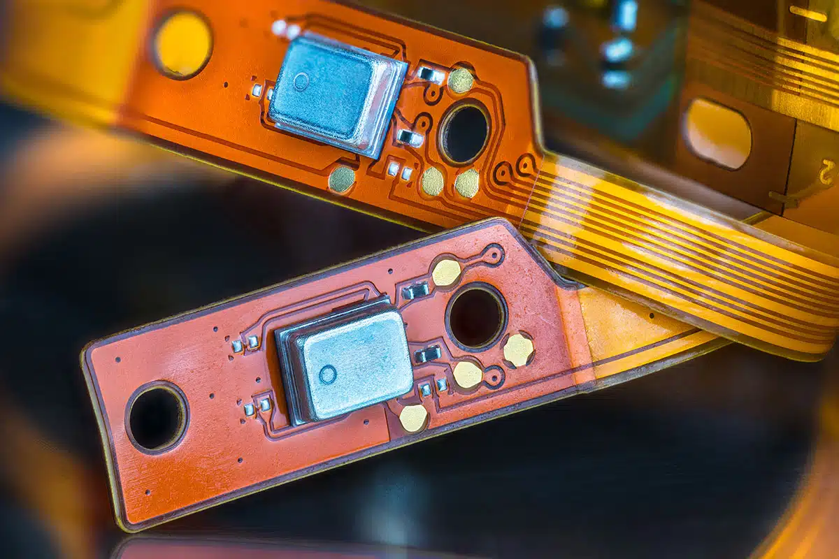
Flexible electronic devices require materials and designs that mitigate the strain and movement that produces unwanted electronic signals. PCBs and their components—especially semiconductors—are becoming more flexible, and origami is inspiring new PCB and device designs that take advantage of this pliability.

To this end, engineers at the University of Illinois at Urbana-Champaign are using kirigami—origami’s sister technique that uses cutting in addition to folding—to produce elastic-like semiconductors that won’t cause troublesome signal outputs. These designs use atomically thin graphene sandwiched between two layers of polyimide to create a highly flexible material, which is then engineered using a kirigami design to further enhance stretchability. These novel semiconductors have proven to be highly strain tolerant and function without producing unwanted motion or signals.

Nanomaterials like graphene are contributing to the next generation of microchips.

In another area of strain engineering (aka “straintronics”), researchers at the University of Sussex have been working with graphene and other 2D nanomaterials to create transistors by using a folding process called “nano origami.” With nano origami, kinks and folds are made in a 2D sheet of graphene—which is itself composed of only a single layer of carbon atoms—to create the smallest ever microchips. These graphene microchips, still in development, will be 100 times smaller than regular microchips. By enabling electronics manufacturers to add dozens of chips to devices without increasing their size or weight, these extremely small microchips seem poised to usher in a new era of electronics.

Self-Assembling Packaging

Perhaps the most obvious application of origami (and kirigami) is in an area that relies heavily on paper and paper-like materials—packaging. With hard plastic losing favor as a packaging material, and with paper and other flexible, organic substances growing in popularity as sustainable substitutes, it’s no surprise that origami is playing an increasingly important role in packaging design.  

One of the most innovative developments in this area is the creation of self-folding packaging, which is adding an efficient new twist to a traditional packaging design—the honeycomb.

Honeycomb structures have all the right properties for good packaging: low weight, effective heat insulation, and high shock absorption. But the folding process has traditionally been time-consuming and impractical, especially for very large or small objects.

That may be changing, however. A group of Japanese scientists have created a packaging design that combines dry paper with wet ink to create a packaging material that folds itself into a honeycomb shape—without mechanical intervention. Best of all, the material can be easily replicated, because what makes this packaging unique isn’t the raw material used to make it, but the pattern of the ink coating that’s applied to the paper.

With this process, low-cost paper is run through an ink-jet printer to coat it with a pre-designed pattern of printing solution. Once the paper comes off the printer, it self-assembles into the desired shape—ready to fit objects of any size.

This yields a sustainable packaging solution that can provide snug cushioning for small or fragile products and absorb shocks and impacts for large unwieldly structures, reducing the risk of damage during transportation.

Future Prospects for Ancient Techniques

From giant telescope mirrors to nano-folded microchips, the art of origami applied to industrial design is set to create more efficient and sustainable products that are cheaper to produce and easier to transport. And with origami techniques just beginning to be utilized for electronics, there are likely many more useful applications for this ancient art that are yet to be discovered.

Electronics Design and Manufacturing Services

Our flexible, customized electronics manufacturing is supported by highly skilled engineers and driven by a commitment to quality and exceptional customer service. From streamlining product designs for greater efficiency, to high-precision manufacturing, to end-of-life product management, our team can help you get the most from your product’s lifecycle.

Thinner boards. More powerful components. Denser layouts. Today’s assembled PCBs are increasingly complex and require thorough and accurate testing to ensure they perform as expected. That’s why, when it comes to getting your product to market, design for test (DFT) is crucial to the manufacturing process. Incorporating DFT principles into the production of your device increases the certainty of your product’s reliability, efficiency, and ultimately, commercial success.

What is Design for Test and Why is It Important?

Testing is an integral part of the electronic manufacturing process. Without it, failure points, power inefficiencies, and reduced functionality in a product can go undetected. Testing can produce valuable system information, providing engineers with opportunities to increase the product’s functionality and performance for the consumer.

Taking the trouble to incorporate DFT principles into your design is an investment that will yield benefits throughout the life of your product.

Designing your electronics device using DFT protocols makes it possible to efficiently and cost-effectively test the product—even after it has been assembled. DFT-savvy engineers can create designs for PCB assemblies that ensure easy testing, with test points that are properly spaced and with enough surface area to give accurate and reliable readings quickly and easily.

Taking the trouble to incorporate DFT principles into your design is an investment that will yield benefits throughout the life of your product—beginning with the detection of design flaws and ending with a satisfied customer.

DFT for Defect Detection

Testing ensures that your product is free of faults and malfunctions and delivers a customer experience that leads to repeat sales.

To ensure a high-quality experience for the end user, it’s important to test your device at multiple stages. Start by virtually testing your design. You’ll want to test each prototype as well, since that’s the best time to work out any real-world issues that weren’t caught during the initial design. Periodic testing should also be conducted during the manufacturing process, to ensure that the product coming off the line is performing to expectations at each stage. 

It can even make sense to test after the sale. If a product is returned from a dissatisfied customer, testing will allow you to find any residual flaws that are affecting your product’s durability or performance. If such a flaw is found, it may make sense to tweak the manufacturing process. Testing will give you the information to determine if the benefits of a manufacturing change will outweigh the costs.

Two engineers, one standing, one seated at a desk, review a board design
A DFT review early in the design process can save you time and money later on.

Provide Data

Recently the engineers at Space X cheered when the Starship rocket spectacularly exploded shortly after takeoff. It seems no one was upset at the sight of billions of dollars’ worth of material and effort going up in smoke. Why? The data. As one of the engineers said: “Success comes from what we learn, and today’s test will help us improve Starship’s reliability.”

Information and data are essential. The benefit of DFT is not just the ability to detect and correct faults, but also to gather critical data that can inform the design of your product’s next iteration. It can allow you to spot weaknesses that can be designed out, or discover ways to increase the power of certain features.

Fortunately for electronics companies, DFT in manufacturing does not require any explosions. But as with space vehicles, it’s important to carefully analyze product failures. Determining what went wrong can yield precious data and allow you to better design your product’s next upgrade. Data gained from DFT can be used to develop new manufacturing procedures, refine features, and produce a more robust product.

Lowering Costs

When manufacturing any electronic product, costs need to be controlled, while quality, durability, and functionality must be maintained. Although testing procedures may initially impact production costs (depending on the complexity of an assembled PCB), testing provides significant savings in the long term. Including test points makes it possible to accurately identify the location and nature of a fault within a system and speeds up troubleshooting. And an experienced engineer can find the optimal placement and use of these test points.

For example, although test points can be located on either the top or bottom of the PCB (so long as they don’t interfere with other electromechanical components), having them on both sides requires the manufacturer to create a clamshell fixture. This approach is expensive, and less accurate than the ideal.

Usually, the better testing strategy is to put test points on one side only. This not only avoids the costs of the clamshell, but also increases accuracy, which in turn enables better batch quality prediction and a fast production time.

Incorporating DFT principles early in the design process will allow you to reap these and other benefits right from the start. Planning for testing, for example, allows you to avoid the expense of adding additional test points later in the production process once it’s become clear that they’re needed.

Compliance and Customer Satisfaction

Most consumers are unaware of the complexity of the assembled PCBs that power their products. But that doesn’t mean their expectations of quality and functionality are low. And of course, manufacturers and OEMs want safety and the very best quality for their customers.

Design for testability is not just about improved functionality and streamlined production. Safety, quality, and customer satisfaction are also key areas that can be improved with DFT. Standards and regulations required by governing agencies are built into the tests that each product must go through.

Even the simplest design has to comply with standards from numerous bodies, both state and federal. And if a device fails to meet regulatory standards, it will be much easier to discover the cause if the product was designed with testing in mind. In that case, it’s a straightforward process to determine which component failed, or which usage scenario created excess stress on the product—or worse, compromised safety or quality. A problem that is identified quickly can be rectified quickly.

Design for Test and for the Future

Electronic devices continue to evolve, as do the PCBs that form their backbone. Flexible PCBs, with their high heat resistance, are becoming more popular for wearable electronics and medical devices. Another trend in PCB construction is the use of biodegradable materials, spurred by consumer demand for greater sustainability. And in a related development, 3D printing—which produces less waste—is also making inroads into PCB production.

And as PCBs change, so will the ways to incorporate test points and other features that allow for the quick detection of flaws or failures. But what’s unlikely to change is the need to test both prototypes and finished products to ensure the best possible consumer experience.

Boards and components will continue to evolve, but the need for testing won’t go away any time soon.

DFT Expertise You Can Rely On

Not sure how to incorporate DFT into your design process? Our highly skilled SMTA-certified engineers are experts in DFT and in all aspects of quality electronics manufacturing. We offer a full range of testing capabilities on site, including 3D X-ray, flying probe test, ICT, conformal coating, functional testing, automated programming, and automated optical inspection (AOI). From streamlining PCBA testing to end-of-life product management, our team can ensure that the products you deliver to your customers meet the highest standards.