For decades, PCBs have used essentially the same configurations to serve the internet application needs of big tech companies. Whether supporting a search engine like Google or an email application such as Microsoft Outlook, traditionally designed and assembled PCBs have been sufficient. Now, however, the increasing reliance on AI is rapidly driving new requirements for PCBs, including the need for new types of components. Designing boards advanced enough to keep up with the demands of AI technology—AI PCB design—is redefining electronics manufacturing.
How AI is Driving Changes in Computer Design
Gordon Moore first posited his famous law in 1965, then updated it ten years later. Since then, Moore’s Law—that the number of transistors in an integrated circuit (IC) doubles about every two years—has been the most famous (if not most important) truism driving the electronics industry. AI is about to change that.
Manufacturers who understand the unique challenges of AI PCB design, as well as appropriate solutions, will be better prepared to ride the AI wave.
According to OpenAI, the amount of computing power—aka “compute”—used for training the largest AI models has been increasing exponentially since 2012, growing 10-fold every year compared to the doubling of chip transistors every two years per Moore’s Law.
This rapid growth is making AI models smarter, but it also requires more energy and resources, posing challenges for sustainability and infrastructure. For example, one ChatGPT query, on average, takes 10 times the electricity to process as a Google search. And while traditionally a single server was sufficient for AI tasks, modern AI applications require global data centers. In fact, by 2026, AI operations could consume over 40% of global data center power, according to Deloitte.
“AI’s transformational potential is analogous to paradigm-shifting technologies like the advent of the internet or the mobile phone, and it has the potential to touch every sector of global industry,” according to a 2023 U.S. Data Center Market Overview by Newmark.
So, what does this AI revolution mean for electronics manufacturers? A lot. PCBs are at the heart of AI hardware, providing the platform that integrates the various components essential for AI systems—processors, memory modules, sensors, and interfaces. Therefore, PCB designers play a crucial role in tailoring the layouts of these boards to meet the specific requirements of AI applications in terms of scalability, efficiency, and performance. Manufacturers whose designers understand the unique challenges of AI PCB design, as well as appropriate solutions, will be better prepared to ride the AI wave.
Challenges in AI PCB Design
A PCB designed to meet the needs of AI will be substantially different from a traditional PCB. AI-focused PCBs are more complex and need to be able to handle more: more component density, more layers (to accommodate dense routing), more data being processed, more frequency, etc. All this complexity creates significant challenges, requiring engineers to design architectures that optimize power consumption while also accounting for heat dissipation, signal integrity, and other factors.
High Density and Complexity
A PCB built for AI applications is more complex and denser than traditional PCBs. It is also likely to have a much higher layer count to allow for more intricate designs and the ability to include more components.
High-Frequency Requirements
To enable rapid data transfer and processing, AI applications often operate at frequencies above 1 GHz. PCBs designed for AI apps must therefore be able to handle high-frequency signals with minimal loss and distortion.
Thermal Management
The high performance requirements and massive data processing of AI applications generate a lot of heat. Properly managing this heat is critical to the performance, reliability, and lifespan of the PCB and its individual components.
Rapidly Advancing Technology
The exponential growth of AI is creating a large demand for PCBs capable of meeting the technology’s requirements. At the same time, manufacturers are scrambling to keep up with the latest AI standards and technologies. This constant need for innovation, combined with the demand for large-scale production, requires product manufacturers to creatively balance product quality and cost efficiency.
Given the engineering and production demands of rapidly advancing AI technologies, what are some ways that product manufacturers can meet these challenges? Here are five best practices to keep in mind when it comes to AI PCB design.
Choose Components Carefully
Be selective in choosing the components to include on AI PCBs, since they determine the functionality and performance of the board. AI algorithms have unique demands, requiring high-performance computing, large data storage, and accurate data acquisition. This is why, as AI hardware has evolved, new components have been developed to meet this technology’s demands, like the accelerator chips that are essential for carrying out the autonomous processes that AI applications rely on.
Unfortunately, there is only so much room on a board. One creative solution to this problem of limited space has been to repurpose existing components. Silicon Valley chipmaker Nvidia, for example, has found that the graphics processing units (GPUs) it developed to render graphics in video games is well suited to the demands of AI.
While computer manufacturers have relied for nearly 50 years on the central processing unit (CPU)—a single, do-it-all chip—it turns out that GPUs are better for AI tasks. Why? A GPU outshines the jack-of-all-trades CPU in performing the simple math that powers the neural networks of AI. In the time it takes a CPU to do a single calculation, a GPU can perform thousands, allowing AI’s neural networks—the basis of chatbots and other AI technology—to analyze significantly more data. By running millions of calculations, they allow a computer to “think” about a problem rather than just calculate simple data.
Joining GPUs, CPUs, and memory chips on the board are sensors and application-specific integrated circuits (ASICs). Unlike the more general-purpose CPU and GPU chips, ASICs are custom designed for a specific application. For example, a smartphone might use an ASIC chip for power management tasks such as battery charging control, display backlight regulation, and power distribution.
With the demands of AI making the PCB ever more crowded, manufacturers should choose the most efficient components for specific tasks. Likewise, careful component selection early in the design phase, a long-established design for manufacturability (DFM) best practice, will make it easier, more efficient, and less expensive to manufacture a board.
Address Thermal Management
Due to intense computational demands and power consumption, AI hardware generates significant heat. Therefore, it’s imperative to design a thermal management system to dissipate heat effectively and quickly. Failure to do so can lead to solder joint failure, delamination, and thermal runaway—a self-reinforcing cycle where components draw more current as they heat up.
Thermal runaway poses significant safety concerns, especially in applications like electric vehicles, consumer electronics, and energy storage systems. For example, if cooling fails in an electric vehicle, localized overheating may cause a sensor failure—resulting in a crash, and possibly a fatality.
One way to address overheating is with proper materials. The most common material used for PCBs is FR-4, a composite of woven glass fabric and epoxy resin. While FR-4 offers dielectric strength and good mechanical properties, and has traditionally been adequate for most applications, it’s not as effective for the high-frequency operations required by advanced AI applications. This has led to the increasing use of a different type of board. Metal Core PCBs (MCPCBs), which use metal substrates, dissipate heat more effectively than traditional FR-4 boards.
Of course, PCBs don’t operate in isolation—they are part of a computing environment that includes external methods for controlling heat, such as fans, heat sinks, thermal pads, and liquid cooling. Therefore, PCB designers need to account for the end application, i.e., make allowances for the ambient temperature and airflow of the environment where the PCB will eventually operate.
Use Rapid Prototyping
Another way to meet the challenges of AI is through rapid prototyping. AI engineers need to experiment with different designs and repeatedly test their AI algorithms, and time is of the essence. Through rapid prototyping, manufacturers can achieve the quick turnaround time for board design and development that AI demands.
Traditionally, it could take weeks or months to design a PCB, test it, adjust it, and then reprint it for validation. Now that process can be completed in days. By drastically reducing the time from concept to functional prototype, rapid prototyping allows manufacturers to more efficiently and economically produce PCBs.
Improve Signal Integrity
AI systems rely on chips that process huge amounts of data at lightning-fast speeds. Because of this, it’s essential to design boards that facilitate clean signals. Here are four ways to ensure high signal integrity on PCBs.
Optimal Trace Design
Designing a PCB trace to maintain signal integrity is much like designing a freeway. Just as a gentle curve on a road allows for smooth traffic, especially at high speeds, gentle bends in a PCB trace will allow for better signal flow. Therefore, sharp 90-degree bends in traces are discouraged when designing for high-speed and high-frequency applications. A more gradual bend of 135 degrees, or even an arced curve, will enable a smooth transition.
Shielding
Just as noise-canceling headphones can protect your listening experience, a good PCB design can protect signals from outside interference. Surrounding signals with a special metal layer, a technique known as shielding, keeps signals clean and protected from electric noise.
Termination
In the same way that bowlers want to keep bowling balls from bouncing back down the alley, PCB designers want to prevent signals from bouncing back at the end of their paths. Bowling alleys use pit cushions to prevent bounceback; a good PCB design employs the appropriate resistors to absorb signal energy.
Filtering
Filtering is just what it sounds like—dampening unwanted parts of a signal, much in the same way a water filter removes impurities. In board design, this means placing the right components, such as capacitors and inductors, strategically near noise sources or sensitive areas, thereby suppressing interference before it spreads across the board.
Optimize PCB Layout
Another important factor affecting AI PCB design is the layout. Carefully selecting the physical arrangement of the components and traces on boards is especially important for AI applications, as AI requires complex and dense layouts, often involving many components, multiple layers, and numerous vias to allow signals to travel between those layers.
Designers must also account for the electrical, mechanical, thermal, and ergonomic requirements of the layout. For example, a key consideration in ergonomic design is flexible PCBs, a quality that is especially important in wearable technology and medical devices that have size and weight constraints.
The Future of AI PCB Design
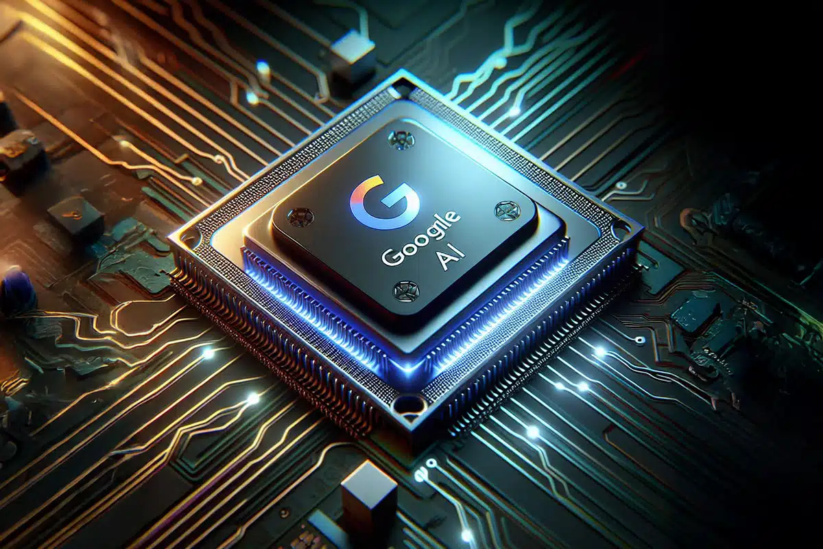
While processing units will remain an integral part of the PCB for the foreseeable future, the units themselves are evolving. Although GPU chips have a leg up on CPU chips, some companies are going further by developing their own chips. For example, Google has designed an AI chip known as a Tensor Processing Unit (TPU). This unit is an application-specific integrated circuit (ASIC) designed to accelerate machine learning tasks, particularly for neural networks. Unlike GPUs and CPUs, these TPUs are specifically optimized for high-volume, low-precision applications, making them ideal for deep learning model training.
Designing its own chips has brought Google several advantages. These include lessening the company’s dependence on chip manufacturer Nvidia; lowering Google’s costs for large-scale AI deployments; and allowing for more customization specific to Google’s AI workloads.
Other tech giants, such as Amazon, Apple, and Microsoft, are also developing proprietary chips, shifting away from traditional manufacturers like Intel. Some experts predict it’s only a matter of time before smaller companies follow suit. As AI continues to evolve, AI PCB design will require more specialized components, flexible boards, and creative engineering solutions to meet the growing computational demands of AI applications.