It happens instantaneously. And if it doesn’t, the consequences range from vaguely annoying to downright alarming. When we touch a screen, drive a car, or use a critical medical device, we expect and rely on instant responses, generated in fractions of a second, for our entertainment and—more and more—our health and safety. And because of the vital role that electronic devices have in our lives, electronics testing and inspection can literally be a matter of life or death. As melodramatic as that sounds, the reality is when it comes to our reliance on electronic devices, rigorous testing of their PCB brains is critical to prevent failures and increase quality.
While it’s easy to see the importance of electronics testing, the question is: When bringing an electronic product to market, what are the tests and inspections you should discuss with your contract manufacturer? Having some insight into what the key tests are can be helpful. So, let’s take a more detailed look at the tests and inspections that electronic devices need to go through.
Devising the best testing strategy will mean working with a manufacturing partner experienced in both DFM and DFT.
What Electronics Testing Will My Product Need?
Although there is value to every test, not every test will be suitable for your product. The when-and-what of testing will depend on several factors, such as the product’s function, user environment, and production volume. The key to success is implementing strategic, device-specific testing that provides thorough quality control, while allowing for streamlined and efficient assembly and production.
The primary uses of the device you want to bring to market will naturally influence electronics testing. A consumer product that sits on a shelf will not encounter the same conditions as a device for the medical or aerospace industry. Electronics subject to harsher environments require stringent test protocols that will challenge stress limits and therefore ensure reliability.
Another consideration is the product’s stage of development. In the prototyping stages, functional and design verification tests are essential for identifying technical flaws and refining the product’s features. The small-batch nature of prototyping, especially rapid prototyping, will inevitably mean different test considerations. While cost-effective at mass production, the expense of some test setups is just not viable for small runs.
Devising the best testing strategy will mean working with a manufacturing partner experienced in design for manufacturability (DFM) and design for test (DFT). An electronics manufacturing services (EMS) provider who understands your priorities can ensure pertinent tests and inspections are conducted to refine the board for optimum safety, quality, and production.
What kind of electronics testing will ensure optimal performance and reliability for your particular product? Here are five of the most robust testing technologies to consider.
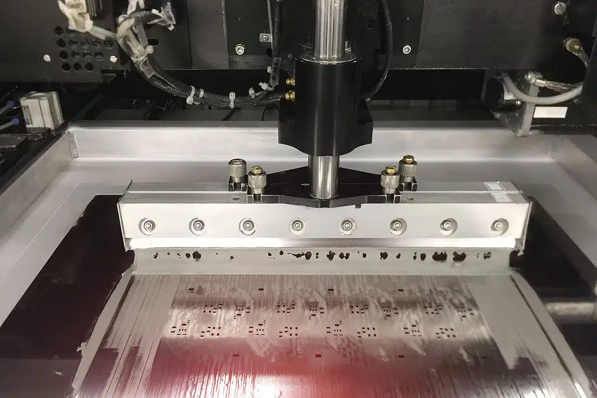
Solder Paste Inspection
Solder paste printing is the first stop for circuit board assembly, and inspecting the solder paste print before the assembly is soldered in the reflow oven is an excellent time for easy preventative fixes. Given that studies show that as much as 70% of all defects on PCBAs come from improper solder paste printing, solder paste inspection (SPI) is an essential step in PCBA production.
Inspection and evaluation of solder paste printed boards can be done using 2D or 3D X-ray imaging. Both will evaluate solder paste coverage, but with the use of a laser, 3D testing will also provide coverage and paste volume data. Since solder paste volume has been linked to long-term joint reliability, 3D imaging is often the preferred quality control method.
Properly implemented, and with the aid of experienced SMT engineers monitoring the process, SPI will improve yields and save money by identifying and correcting solder paste errors early.
SPI is useful in both the development (prototyping) and in-process stages of production. In addition to spotting solder print defects (insufficient paste, bridging, etc.), solder paste inspection will gather information on printing consistency and volume, providing valuable statistical analysis that can guide design improvements.
Automated Optical Inspection
Optical inspections are a critical form of testing. Even traditional optical inspections, whether done by the naked eye or with the aid of magnifying glasses and microscopes, yield valuable information—especially when performed by experienced engineers and technicians. But today’s PCBAs, with their highly complex grid arrays and micro-sized components, also benefit greatly from the accurate and efficient capabilities offered by automated optical inspection (AOI).
With a camera system capable of capturing 2D or 3D images, AOI machines scan a PCBA and compare the images to parameters and reference images in the design database. This allows the system to detect missing components, incorrect components, skew or misalignment, and other visually identifiable defects. Any defects that are discovered can then be flagged and pulled for further inspection or rework.
Although 2D camera and sensor quality are equal to that of 3D imaging on AOI machines, 2D imaging is limited to evaluating visible components. With 3D X-ray, defects in hidden areas of integrated circuits can be identified. 3D X-ray can take longer and may come with an added cost, but with component interconnects becoming smaller and boards more compact, it’s often the best choice for especially complex PCBAs and devices.
AOI systems are highly versatile, and so are typically used at more than one stage of the manufacturing production line. Their use pre- and post-reflow is common, depending on the board and the types of defects that must be avoided. Your EMS provider will help you decide where AOI fits into your device manufacturing process by considering your production volume and rate, as well as the defects that are essential to avoid.
Flying Probe Test
While vital inspections such as SPI and AOI check defects on a board’s surface, component placement, and stability, a flying probe test (FPT) assesses and verifies the functionality of individual components on the PCBA. Discovering flawed components means they can be pulled and replaced before creating device failures.
To do this, probes “fly” over the soldered board on high-speed gantry mechanisms, and conduct a programmed test sequence set up by SMT engineers in accordance with the specific requirements of the device under test (DUT). Without powering up the board, the FPT conducts its test with as many as 20 moving probes that check individual components. The probes test parameters such as voltage measurements, shorts, opens, bad contacts, and diode issues.
Because the FPT is considered “fixtureless,” it does not come with high tooling expenses—a cost-saving benefit that can make it an ideal choice for prototypes and small to medium production volumes.
In-Circuit Test
While FPT is useful for small volumes, the in-circuit test (ICT) fixture—which uses the same methodology (testing individual components) as the FPT—can be a good choice when it comes to products that are fully developed and in production at high volume, due to its very short test time compared to FPT.
As test fixtures, ICTs require DFT-savvy engineers to incorporate the test points in the board and use custom tooling to build the fixture. Creating the fixture naturally comes with upfront tooling costs, which can make it prohibitively expensive for prototyping, but for higher volume runs this cost is offset by the lowered expense of streamlined production. An ICT fixture can lower the per-unit cost significantly—by as much as ten or more units for every one unit that the FPT processes.
Functional Circuit Test
As the final step of electronics testing, the functional circuit test (FCT) fixture does just what it says on the box: test the device’s functionality. This test provides a pass/fail determination of the DUT’s functionality, validating the device’s design and implementation. The test is conducted by simulating the operating environment that the product will be used in, ensuring the board functions as intended, and is free of errors.
In addition to design flaws, FCT can spot both manufacturing defects and software bugs that might affect the device’s performance. It can also show whether the device adheres to all relevant standards and specifications. For critical devices, such as medical equipment or automotive systems, functional testing is crucial for ensuring safety and reliability, and so a series of FCTs may be necessary. This is where thorough testing helps verify that the device operates correctly, reducing the risk of malfunctions or complete failure.
Driving Innovation and Building Trust
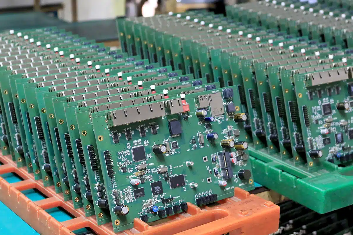
Whether they’re in consumer devices designed to entertain, or medical devices created to save lives, complex PCB assemblies with small components demand rigorous testing and inspection. Comprehensive testing ensures that electronic devices meet design specifications, adhere to industry standards, and deliver optimal performance.
It’s also true that the process of electronics testing not only ensures quality, it also drives innovation. By providing comprehensive, detailed feedback, testing enables iterative improvements that lead to cutting-edge advancements and enhanced user experiences.
That’s why it’s more important than ever for manufacturers to embrace robust testing practices. Ensuring high performance and reliability enables electronics companies to establish trust with customers, maintain a competitive edge in the market, and build a reputation for excellence.